Pattern Transfer: Photolithography Practice

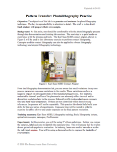
This 3-page lab guide, created by the Nanotechnology Applications and Career Knowledge Support (NACK) Center at Pennsylvania State University, is for a photolithography lab activity. During the lab, students will use 3'' silicon substrates to "evaluate three different exposure times using hard (standard) contact" to then "decide which exposure time yields the best feature resolution from the results of the experiment." The lab guide includes a description of the lab, background information, pre-requisites for completing the lab, lab instructions, and 11 student questions.
About this Resource
Publisher
Date Issued
September 4th, 2009
Resource Type
Format
Audience
Education Level
Language

Subject
ATE Area
GEM Subject
Subject
Relation
Is Related To
Associated Files
Archived
STEMLink
Available in STEMLink

Comments