Lecture 14: Printed Circuit Board Design (Ki-CAD)
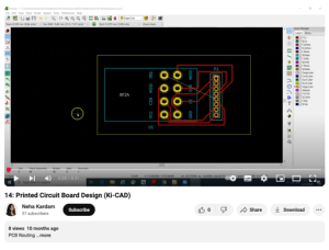
This video was created by Neha Kardam and is part of a series of lectures on printed circuit board (PCB) design using Ki-CAD software. This lecture covers the fundamentals of routing connections between pins. Kardam demonstrates how to create edge cuts using the correct layer and explains the process of routing while avoiding crossing connections. An example of routing between two pins is shown. The video also shows a demonstration of running an electrical design rule check (DRC) and reviewing the messages displayed.
This video runs 4:31 minutes in length. Additional videos from the series are available to view separately.
About this Resource
Creator
Publisher
Date Issued
March 19th, 2024
Resource Type
Audience
Education Level
Language
Subject
GEM Subject
Subject
Relation
Associated Files
Archived
Rights
Access Rights
STEMLink
Available in STEMLink
Comments