Lecture 19: Printed Circuit Board Design (Ki-CAD)
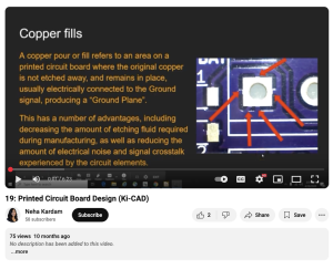
This video was created by Neha Kardam and is part of a series of lectures on printed circuit board (PCB) design using Ki-CAD software. During this lecture, Kardam provides an overview of copper fills and demonstrates how to add them to a schematic design. The copper zone properties are modified and the fill is connected to a specific net. Kardam concludes by showing how to inspect and verify the design for proper connections.
This video runs 6:23 minutes in length. Additional videos from the series are available to view separately.
About this Resource
Creator
Publisher
Date Issued
March 19th, 2024
Resource Type
Audience
Education Level
Language
Subject
GEM Subject
Relation
Associated Files
Archived
Rights
Access Rights
STEMLink
Available in STEMLink
Comments