Browse Resources
Resources |
|---|
 This webinar, published by the Nanotechnology Applications and Career Knowledge Support (NACK) Center at Pennsylvania State University, focuses on the construction of a simple microelectromechanical systems (MEMS) pressure sensor. During the Webinar, Dr. Matthias Pleil from the University of New...
 This webinar, published by the Nanotechnology Applications and Career Knowledge Support (NACK) Center at Pennsylvania State University, covers the fabrication and characterization of nanostructures using atomic force microscopy (AFM). During the Webinar, Dr. Wesley Sanders from Salt Lake Community...
 This presentation, published by the Support Center for Microsystems Education (SCME), took place at the Micro Nano Technology Education Special Interest Group (MNTeSIG) Live 2021 conference. In the presentation, Neda Habibi explores self-assembling molecules and how they create nanostructures....
 This poster presentation, published by the Support Center for Microsystems Education (SCME), took place at the Micro Nano Technology Education Special Interest Group (MNTeSIG) Live 2021 conference. In the presentation, Wesley McIver outlines recommendations and operating conditions for micro...
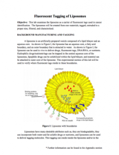 This resource, provided by the Nanotechnology Applications and Career Knowledge Support Center (NACK Center), includes a lab guide and corresponding videos that walk through the process of examining "the liposome as a carrier of fluorescent tags used in cancer identification." Throughout the lab,...
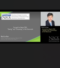 This video, published by the Nanotechnology Applications and Career Knowledge Support (NACK) Center at Pennsylvania State University, covers the focused ion beam (FIB) and its use for preparing materials for sample analysis. In the video, Wook Jun Nam from Pennsylvania State University defines and...
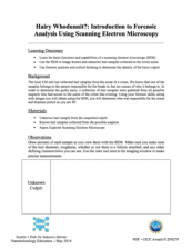 This 3-page activity was created by SHINE: Seattle's Hub for Industry-driven Nanotechnology Education and covers forensic analysis using scanning electron microscopy. In this activity students will learn basic functions and capabilities of a scanning electron microscope (SEM), use a SEM to image ...
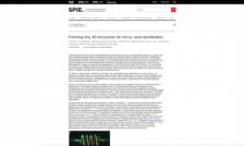 This article from SPIE describes how dielectric breakdown and wet etching may provide a method of fabricating 3D nano- and microscale channels inside transparent dielectric materials. The article includes several graphics which help to illustrate the concept.
 Material from this website was produced as part of a 4-part ten hour course designed to introduce users to the basics of nanotechnology. This course includes four sections and additional Nanotechnology essays. Each section of the course may be downloaded as a PowerPoint or PDF, essays may be...
 This webinar, published by the Nanotechnology Applications and Career Knowledge Support (NACK) Center at Pennsylvania State University, provides a brief overview of fourier transform infrared spectroscopy (FTIR) and ultraviolet-visible (UV-Vis) spectroscopy techniques. During the webinar, presenter...
|
| ← PreviousNext → |