Browse Resources
Resources |
|---|
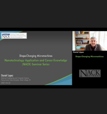 In this webinar, hosted by Nanotechnology Applications and Career Knowledge Support Center (NACK Center), Daniel López from Pennsylvania State University, discusses the evolution and directions of research in micromachines and shape-changing micromachines. Throughout the presentation, López covers...
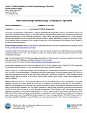 These nanotechnology lab use documents are provided by Seattle's Hub for Industry-driven Nanotechnology Education (SHINE) and cover policies and fees for the North Seattle College (NSC) Nanotechnology Lab. The lab is open to NSC students, academic users, and industry users who complete a 4-hour...
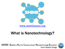 This collection of resources is provided by Seattle's Hub for Industry-driven Nanotechnology Education (SHINE) and includes six nanotechnology PowerPoint lectures. Lectures include Applications of Nanotechnology, Intro to Scanning Electron Microscope, Nanotechnology Characterization, Natnotechnology...
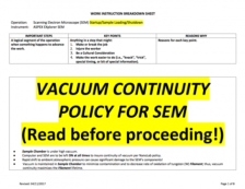 This collection is provided by Seattle's Hub for Industry-driven Nanotechnology Education (SHINE) and includes ten nanotechnology related standard operating procedures (SOPs). SOPs are provided for the following operations: scanning electron microscope, sputter coater, profilometer, atomic force...
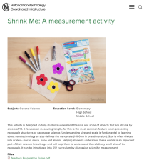 This lesson, presented by the National Nanotechnology Coordinated Infrastructure, covers the general concepts of size and scale by focusing on measuring length. Students will learn about different scales of measure which is fundamental to learning about nanotechnology. After all, "helping students...
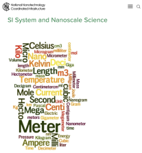 This lesson, presented by the National Nanotechnology Coordinated Infrastructure, covers the metric system. Students will explore the use of the metric system in the activities, and also "read the How Stuff Works article –“How Nanotechnology Works” and answer questions about the article. Further...
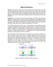 This 3-page document, created by the Nanotechnology Applications and Career Knowledge Network (NACK) Center at Pennsylvania State University, is a guide for a laboratory activity where students "learn about growth of silicon nanowires using the metal-catalyzed vapor-liquid-solid (VLS) processes."...
 This 31-minute video, one of seven in a series on semiconductors, provides a look at the thin-film deposition process. Industrial footage and animation show the chemical and physical reactions used to create the many layers of an integrated circuit. The video includes animations and close-up views...
 One of seven in a series, this 37-minute video provides a look at the etching process as it is used in most production labs today. The video shows how thin films of nonconductive, semi-conductive, and conductive materials are sculpted into microchips by following the various etching processes and...
 This 40-minute video on semiconductor manufacturing shows how microchips are made and how they work in electronic products. The video provides an overview of front-end manufacturing, from crystal growth through design, to the fabrication process of CMOS integrated circuits. The video includes...
|
| ← PreviousNext → |